The host system communicate with the Virtex-5 user FPGA through a local bus interface defined by Alpha-Data. This local bus has its own clock, LCLK. The frequency of LCLK is within the range of 32MHz to 80MHz in the Axel system. This clock is generated from a 200MHz reference by a DC within the bridge Virtex-4 (V4LX25) FPGA.
The user logics taking care of the heavy computing task in the user FPGA usually runs in a different clock domain other than this 80MHz LCLK. This may be the result of a faster core implementation or the using of external DDR2 memory. The memory use another clock from the 200MHz and is usually scaled up to 333MHz using a PLL inside the user FPGA. We use UCLK as the clock for user logic.
Thus there is a need for synchronization between the local bus logics in LCLK domain and the user logics in the UCLK domain. This interface is presented as a 32-entry array of 64-bit registers. This notes presents the synchronization scheme of this register interface. The frequency of UCLK is assumed to be faster than that of LCLK.
To enable data flow from host to FPGA, the byte write enable singal, reg_wr(255 downto 0), is synchronized. The input data, reg_in(63 downto 0), remains in the LCLK domain. These data altered when there is a transfer in the local bus and the current operation is a write operation. User logic will sample the contents of reg_in according to the reg_wr value. The circuit for the reg_wr synchronization is shown in the figure below. This circuit is implemented in the user_reg_sync.vhd file.
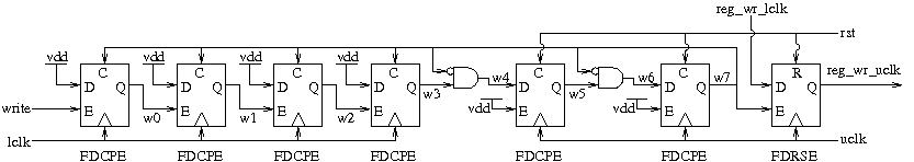
Here the write signal is from the local bus to identify a write operation. The reg_wr_lclk and reg_wr_uclk signals are actually 256-bit in width. The w0 signal is output as busy to the host such that the new operation will be start until the reg_wr signal is stable in the UCLK domain.
To enable data flow from FPGA to host, the data, reg_out(2047 downto 0), is synchronized by copying the contents from the UCLK domain to LCLK domain periodically and automatically. The circuit for this process is shown in the figure below. This circuit is implemented in the reg_sync.vhd file.
